


Editor’s Note – In this series, we will take a behind the scenes look at how an engineer tackles a project from beginning to end. What challenges will come up? How can we face problems and come up with solutions? Aside from project completion, what are successes that we can celebrate along the way?
The Zmod ports on Digilent’s Eclypse Z7 board run on the SYZYGY® specification. SYZYGY® is an open standard designed for the connection and communication of peripherals to FPGA systems using a commodity connector and common electrical specification. In this part of the design process, I have decided to design and manufacture a test board in order to implement and debug compliancy to the SYZYGY® specification. It is extremely important that a staggered approach in electronics design is taken to ensure that the final design has the best possible outcome.
Since the final design will include the RF Front end chip and amplifiers, which is a relatively complicated design, compliancy to the SYZYGY® specification is imperative to ensure that the Zmod peripheral can communicate to the VIO controller via an I2C Bus and hence give way to the carrier controller to set up the VIO voltages for the FPGA and the circuitry on the peripheral for efficient communication.
The main idea of the SYZYGY® specification is to enable fast data transfer for the FPGA to and from the peripheral (In this case the RF Front End Chip, AD9361). The carrier board which in this case is the Eclypse has a VIO controller which has to read data from the peripheral and set the VIO voltage (Vadj) for the FPGA and the peripheral itself. The data stored on the peripheral is called DNA data which includes manufacturer name, part number, serial number, required VIO voltage, LVDS or CMOS data transfer and other information related to the peripheral. The DNA data is stored on a microcontroller on the peripheral, this microcontroller is referred to as a pMCU in the SYZYGY® Specification. The designed test peripheral includes the 40-pin connector used for the peripheral (QSE-020-01-F-D-A), the pMCU (Attiny44a), some LEDs for testing and headers to be able to carry out some additional tests.
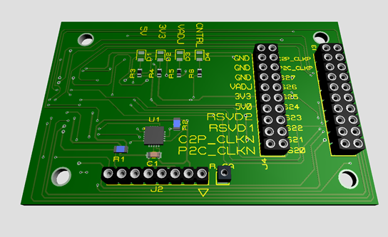
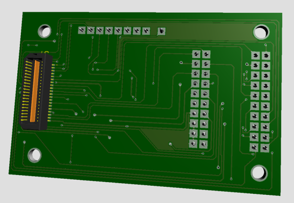
Figures 1 and 2 illustrate the designed test board which will be programmed (Attiny44a) and connected to the Eclypse Z7 for testing. Source code for the SYZYGY® specification can be found on the SYZYGY Github, this will be used as a solid reference for implementation of the test peripheral. Once the test board is manufactured and programmed, various signals will be generated from the FPGA which will be analyzed using the ADP3450 Portable High Resolution Mixed Signal Oscilloscope from Digilent. This will not only help to design a SYZYGY® compatible peripheral, but also provide peace of mind regarding the connections between the FPGA and the designed peripheral. In the next posts I make for Engineers in the Wild, I will actually be running the tests, so make sure to check back!